English


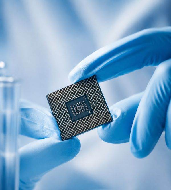
A material long used in the semiconductor industry changes its properties when it is reduced to a thickness of just a few nanometers. Researchers at Lawrence Berkeley National Laboratory have discovered that titanium dioxide (TiO₂), commonly considered a dielectric material, becomes ferroelectric when thinned below 3 nanometers, and the property can be maintained even at thicknesses of about one nanometer. The discovery could pave the way for denser chips, more energy-efficient memories and new electronic devices, without the industry having to abandon manufacturing processes already in use.
• A familiar material, an unexpected property
Titanium dioxide is not an exotic material. It is already used in the semiconductor industry and is well known to researchers and manufacturers. It is precisely this familiarity that makes the Berkeley Lab team's discovery interesting for the electronics industry. Researchers have found that when titanium dioxide films are reduced to thicknesses of less than 3 nanometers, the material undergoes a phase change and acquires ferroelectric properties. According to Berkeley Lab, the effect can be observed even when the film is about one nanometer thick. A nanometer is one billionth of a meter. At this scale, matter can no longer be treated simply as a miniaturized version of the material known at normal dimensions. Reducing the size can change its fundamental structure and properties. In the case of titanium dioxide, this is exactly what appears to be happening.
• What it means for a material to become ferroelectric
Ferroelectric materials have an important property for electronics: they can retain an electrical polarization that can be changed by applying a voltage. This characteristic makes them interesting for memory devices, because information can be associated with stable electrical states. Until now, titanium dioxide was considered, in this context, an ordinary dielectric. But the research at Berkeley Lab shows that drastically reducing the thickness can trigger the appearance of a ferroelectric phase. Basically, the researchers did not discover an entirely new material, but a new property of an already used material. It is one of the situations in which miniaturization not only reduces the size of a device, but can change its very physics.
According to Berkeley Lab, below the threshold of about 3 nanometers, a phase transition occurs through which the crystalline structure of titanium dioxide loses its inversion symmetry and stabilizes in a ferroelectric phase. The phenomenon is important because the property does not have to be obtained by adding an exotic material or through a completely new process.
The researchers made the films by atomic layer deposition, known by the abbreviation ALD (atomic layer deposition), at temperatures below 400 degrees Celsius. Berkeley Lab emphasizes that this process is compatible with processes already used in the manufacture of semiconductors.
This compatibility is one of the most important components of the discovery. In the semiconductor industry, a spectacular physical property is not enough for a material to reach a commercial product. The material must be able to be manufactured at scale, integrated into existing processes and offer stable performance.
• The advantage of an already known material
In this case, researchers start from a material that is already well known to the industry. If the discovered properties can be transformed into a commercial technology, manufacturers would not necessarily have to build an entire manufacturing chain from scratch. Berkeley Lab shows that ferroelectric TiO₂ films remained stable on both silicon and amorphous surfaces. This result is important for integrating the material into different types of devices. The researchers believe that this combination of the material already used in industry and the manufacturing process compatible with existing technologies could lower the barriers to possible future applications.
One of the directions of interest is electronic memory. Ferroelectric materials have long been studied for non-volatile memories, neuromorphic computing devices and other technologies that aim to reduce energy consumption. In the case of titanium dioxide, the potential advantage comes precisely from the possibility of obtaining ferroelectric properties in an extremely thin film. The smaller the components can be made, the greater the potential for integrating a greater number of elements in a limited space. Berkeley Lab believes that the discovery could contribute, in the future, to the development of denser, faster and more energy-efficient memory devices. energy.
• Miniaturization changes the rules
The discovery is part of a broader trend in semiconductor research: As devices get smaller, the behavior of materials becomes increasingly difficult to predict based on their macroscopic properties alone. At nanoscale, interactions between atoms and electrons can significantly alter a material's properties. In the case of titanium dioxide, the researchers identified a structural transition that occurs when the film thickness is reduced sufficiently. The material's structure reorganizes, and this change allows for the emergence of electrical polarization that can be changed by applying a voltage. In other words, reducing the thickness becomes a tool with which researchers can modify the material's properties. The study, conducted by researchers at Berkeley Lab and collaborators, was published in the journal Science.



























 Euro
Euro Dolar SUA
 Franc elveţian
 Liră sterlină
 Gram de aur